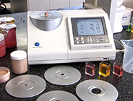
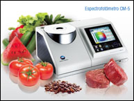
Sabores y Fragancias: Procedimiento de Medición
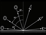
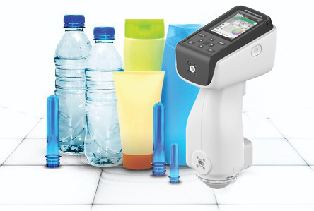
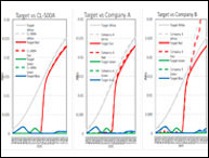
Ha habido un incremento en la demanda de sabores y fragancias con un crecimiento anual estimado de 4.5%. Este crecimiento lleva a incrementar el control en la calidad de sabores y fragancias cuando se analizan parámetros como color, sabor, textura y aroma, entre otros. La medición de color puede ser realizada en varias etapas como ser la etapa inicial de la materia prima, la etapa de elaboración del producto y la etapa del producto terminado. En este documento se mencionarán algunas de las prácticas más comunes usadas en la industria como también los desafíos y soluciones que encuentran los técnicos.