
At SID Vehicle Display Konica Minolta Sensing Americas, Inc. to present a sneak preview of our latest developments in imaging colorimeters and photometers

![]()
Ramsey NJ September 2019 - Konica Minolta Sensing’s Instrument Systems group is pleased to announce that we will be displaying our LumiTop 2700/4000 at SID Vehicle Display and Interfaces 2019 in Livonia, Michigan, booth #65 September 24-25, 2019. We will be also offering a sneak preview of the LumiCam B generation; our latest addition to our imaging colorimeters and photometers line.
Sneak preview at SID
The LumiCam B generation, measures the luminance and color distributions of automotive interior displays 30% faster and easier. This conveniently compact system with a 25% smaller footprint includes new software allowing for controlled, motorized aperture and focus features which allows for both easier and faster measurement setups. To see the debut of the LumiCam B generation model visit Konica Minolta Sensing at SID Vehicle Display table #65.
Lab specs meet production speed with easy integration
On display will also be the LumiTop 2700/4000. This colorimeter combines accuracy with speed through its easy integration into existing production lines, 3-in-1 measurement solutions and the detailed spectral imaging. The LumiTop 2700/4000 spectroradiometer and color meter is tailored for end-of-line (EOL) verification of the latest OEM requirements made on automotive interior displays. The spectrally optimized, high-resolution 2D camera enables fast and precise testing with a total production line testing time of less than 1 second per display!
All in one solution
With LumiTop you can organize different test applications on a single test station, e.g., the evaluation of uniformity and Mura effects, the analysis of white balance, color gamut or contrast ratio, or the measurement of flicker. The LumiTop in combination with the CAS spectrometer provides an ideal measurement solution for a fast EOL testing of main OEM display quality requirements, such as color, uniformity, gamma, and dot defects. The testing time for a complete EOL assessment can be decreased considerably to less than 15 seconds per display.
The LumiTop systems are perfect for use in display production lines or quality control, where the benefits and capabilities of both the accurate spot measurement of spectroradiometers and the lateral resolution of camera measurements are highly valued. Instrument Systems offers the LumiTop in two variants: the LumiTop 2700 with a resolution of 6.1 megapixels and the LumiTop 4000 with a higher resolution of 12 megapixels.
New: LumiTop Ultra-High Resolution
The new ultra-high resolution LumiTop allows pixel level analysis of complete displays in one single shot. This innovative measurement device is thus perfect for fast and accurate quality control and pixel calibration of OLEDs or Micro-LED displays in production lines. An integrated pixel shift mechanism suppresses demosaicing artifacts by true full color measurements and even provides increased resolution of 600 megapixels per color channel, which makes this device also very valuable for research and development.
On-site presentation at SID-Vehicle Display
An onsite presentation entitled, "End of Line Testing of Recent Display Quality Standards" will be given by our fellow colleagues from Instrument Systems GmbH on Wednesday, September 25th from 9:15 am-9:35 am.
Further information can be found on our website: https://sensing.konicaminolta.us/us/products/lumitop-2700-lumitop-4000-spectrally-optimized-luminance-and-color-measurement-camera/
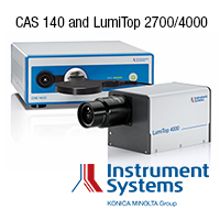
Figure: Spectrally enhanced imaging colorimeter-combines accuracy of CAS140CT/D with the advantages of imaging colorimetery.
Company profile of Konica Minolta Sensing Americas
Konica Minolta Sensing Americas, Inc. (KMSA), a wholly owned subsidiary of Konica Minolta, Inc., Sensing Business Unit is recognized as the international leader of industrial color and light measurement. The company is responsible for product lines that continuously revolutionize how visual perception is measured by the world.
Konica Minolta Sensing Americas' Ramsey, New Jersey corporate headquarters is fully equipped with a state of the art service center, technical support center, and a focused sales force dedicated to both the North American and South American regions. When it comes to color and light measurement, the world looks to Konica Minolta.
USA Contact:
Peter Roos, Marketing Manager
Konica Minolta Sensing Americas
Phone: (201) 236-4300
Toll Free: (888) 473-2625
Web: https://sensing.konicaminolta.us/us
Email: marketing.sus@konicaminolta.com
Company profile of Instrument Systems GmbH.
Instrument Systems, founded in 1986 and based in Munich, Germany, develops, manufactures and markets turnkey solutions
for light measurement. Its main products are high-performance array spectroradiometers, imaging photometers and colorimeters. Key applications are LED/SSL and display measurement, as well as spectroradiometry and photometry. Today Instrument Systems is one of the world’s leading manufacturers in this area. Products of the Optronics line for the automotive industry and transport sector are developed and marketed at the Berlin location. Since 2012 Instrument Systems has been a wholly-owned subsidiary of the Konica Minolta Group.
International Contact:
Dr. Karin Duhnke, Instrument Systems GmbH
Web: https://www.instrumentsystems.com
Email: duhnke@instrumentsystems.com
Terms and product names may be trademarks or registered trademarks of their respective holders and are hereby acknowledged.
August 2019


/Blog_300x200px-MeasureLuminance-LightMeters.jpg?width=300&name=Blog_300x200px-MeasureLuminance-LightMeters.jpg "Blog_300x200px-MeasureLuminance-LightMeters")


/300x200px_CAS140-LumiTop.jpg?width=300&name=300x200px_CAS140-LumiTop.jpg "300x200px_CAS140-LumiTop")
/300x200px_CAS140CTHR-ISlogo.jpg?width=300&name=300x200px_CAS140CTHR-ISlogo.jpg "300x200px_CAS140CTHR-ISlogo")
June 2019
|
||||||||||||||||||||||||||||||||||||||||||||||||||||||||||||||||||||||||||||||||||||||||||||||||||||||||||||||||||||||||||||||||||||||||||||||||||||||||||||||||||||||||||||||||||||||||||||||||||||||||||||||||||||||||||||||||||||||||||||||||||||||||||||||||||||||||||||||||||||||||||||||||||||||||||||||||||||||||||||||||||||||||||||||||||||||||||||||||||||||||||||||||||||||||||||||||||||||||||||||||||||||||||||||||||||||||||||||||||||||||||||||||||||||||||||||||||||||||||||||||||||||||||||||||||||||||||||||||||||||||||||||||||||||||||||||||||||||||||||||||||||||||||||||||||||||||||||||||||||||||||||||||||||||||||||||||||||||||||||||||||||||||||||||||||||||||||||||||||||||||||||||||

/300x200px_Blog-VirtualReality.jpg?width=300&name=300x200px_Blog-VirtualReality.jpg "300x200px_Blog-VirtualReality")

/300x200px_IS-Multi.jpg?width=300&name=300x200px_IS-Multi.jpg "300x200px_IS-Multi")

Subpixel Metrology of microLED and AR/VR Display Applications
![]()
An ultra-high resolution version of the LumiTop, known as a spectrally enhanced imaging colorimeter with unprecedented accuracy for high speed 2D measurements, will be presented by Instrument Systems at the Display Week I-Zone 2019.
May 2019 - Konica Minolta Sensing Americas, Inc. and Instrument Systems GmbH will focus the spotlight at Display Week Exhibition in San Jose, CA from May 14 - 16 on applications representing the major trend in the display industry: more pixels. LEDs are a strong candidate for the realization of very high display resolutions with pixel sizes as small as 10 µm and equally small pixel pitches. A higher resolution means that imaging light measurement devices must advance accordingly. Within its LumiTop series, Instrument Systems developed an ultra-high-resolution camera with an extraordinary technical design and outstanding measuring portfolio for unprecedented accuracy and high speed 2D measurements. In the Innovation-Zone of the Display Week Exhibition the light measuring device will be presented in an application for display testing in production lines where tact times are extremely short. At booth #1528 the LumiTop is showcased with a head-mounted display to be measured as innovative AR/VR display application. Additionally, high-end measurement systems for quality control, automotive applications, and production testing will be presented by our light measurement experts.
The ultra-high resolution LumiTop model merges a 150-megapixel camera with the high-end spectroradiometer CAS-140D. Using the extremely accurate spectral information of the CAS-140D measurements as live reference guarantees spectroradiometric test accuracy across the whole image of the camera. The resolution of 150 megapixels thereby allows (sub-)pixel level analysis of complete displays in one single shot. This measurement device is thus perfect for very fast and accurate quality control and pixel calibration of OLEDs or LED displays in production lines. Many different test applications can be organized in a single test station, as, e.g., the evaluation of display uniformity, pixel defects, white balance, color gamut, contrast ratio or the measurement of intensity modulations. Notably,
the LumiTop can be equipped with a fast photometer for flicker or luminance modulation measurements.
For mixed reality technologies (AR/VR) the LumiTop is the perfect system in R&D labs. These innovative display applications require more, i.e. smaller pixels with higher fill factors. Luminance and color variations between pixels and subpixels are likely and strongly influence the visual quality of displays. Augmented reality glasses or virtual reality head-mounted displays are close-fitting to the observer’s eye. Thus, screen-door effects and pixel non-uniformities are easily visible and disturbing to the consumer. To
meet this high standard Instrument Systems GmbH developed the LumiTop series. An integrated pixel shift mechanism suppresses de-mosaicing artifacts by true full color measurements and even provides increased resolution of 600 megapixels. The product is integrated in Instrument Systems’ comprehensive new software “LumiSuite”, which comes with a user-friendly GUI for laboratory applications and a powerful software development kit allowing an easy implementation into any production line. Konica Minolta Sensing will be displaying its CA-410 Display Color Analyzer with its Type C probe with it’s ability to conform to the new color-matching functions for CIE 170-2:2015. Users can more accurately measure and adjust the chromaticity and white blance of dsplays that have a wide color gamut. Used for high-speed measurement on precise luminance, chromaticity and flicker of HDR displays including curved OLED screens.
Among these highlights more advanced lighting technology will be demonstrated at several photometric and spectroradiometric measuring stations at Display Week booth #1528:
High-power LED and LED Testing
Instrument Systems will show a complete light measurement setup with the high-end array spectroradiometer CAS-140D and the positioning station DTS-140. As the entire spectrum is captured simultaneously, very short measuring times can be achieved in the order of milliseconds with highest measurement accuracy. This makes the solution ideal for the characterization of low-lumen or LEDs. Typical application areas are display production and automotive interior lighting.
VCSEL Testing
The design of the recently launched spectroradiometer CAS 120B-HR of Instrument Systems is geared to the measurement of narrow-band emission sources e.g., laser diodes (also VCSEL). An exceptionally high spectral resolution of up to 0.12 nm full width at half maximum and particularly short integration times as low as 4 ms enable fast tests in the lab and production. Time-resolved measurements of laser diodes with a pulsed operating mode in the nanosecond range are also possible in an expanded setup with a
photodiode. Demo measurements and evaluations are presented at the booth.
Goniometric Display Measurement
Using the established DMS 803 display measurement system, Instrument Systems experts will be giving live demonstrations of the diverse possibilities of viewing angle dependent display analysis: motorized positioning unit, temperature chamber of -40 to +105°C, measurement of the spectral reflection value under direct/diffuse hemisphere lighting, determination of the contrast of OLED and LCD displays with different types of ambient light, etc. The latest features allow a qualification of curved displays.
We invite you to discuss your special measurement tasks with our experts at our booth and also to listen to Instrument Systems and Konica Minolta Sensing Americas’ expert lectures:
“Display Metrology: Basics, Framework, and Applications”
Monday, May 13 / Session 06 / 10:20 - 11:50 AM / Room LL21ABC
Speaker: Michael Becker, Instrument Systems GmbH Munich Germany
“Evaluating VR/AR and Curved OLED Screens using New Progressive Technological Instruments”
Tuesday, May 14 / Session F2.2 / 2:15PM / Executive Ballroom
Speaker: Jay Catral and Randy Klimek, Konica Minolta Sensing Americas, Ramsey, NJ
“Flicker from Electronic Displays: Reconsidering the Confusion”
Thursday, May 16 / Session 50.1 / 09:00 - 10:20 AM / Room LL20A
Speaker: Michael Becker, Instrument Systems GmbH Munich Germany
Co-Chair: Jürgen Neumeier, Instrument Systems GmbH, Munich, Germany
“OLED vs. LC Displays - The Race toward Rec. 2020 and HDRI”
Friday, May 17 / Session 83.1 / 10:40 - 11:00 AM / Room LL20A
Speaker: Michael Becker, Instrument Systems GmbH Munich Germany
Further information can be found on the following websites:
Konica Minolta Sensing’ website: https://sensing.konicaminolta.us/us/applications/instrument-systems/
Instrument Sytems website: http://www.instrumentsystems.com/
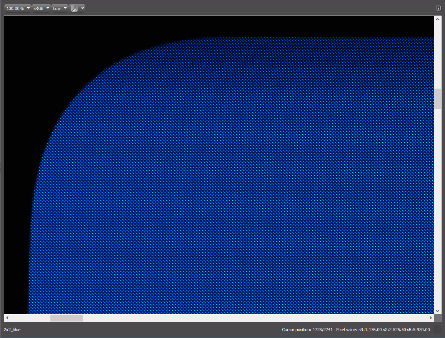
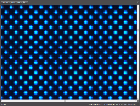
Figure: Zoomed-in measurements of an OLED display measured with the prototype of LumiTop UHR to be shown at the Innovation-Zone.
Company profile of Konica Minolta Sensing Americas
Konica Minolta Sensing Americas, Inc. (KMSA), a wholly owned subsidiary of Konica Minolta, Inc., Sensing Business Unit is recognized as the international leader of industrial color and light measurement. The company is responsible for product lines that continuously revolutionize how visual perception is measured by the world. Konica Minolta Sensing Americas' Ramsey, New Jersey corporate headquarters is fully equipped with a state of the art service center, technical support center, and a focused sales force dedicated to both the North American and South American regions. When it comes to color and light measurement, the world looks to Konica Minolta.
USA Contact:
Peter Roos, Marketing Manager
Konica Minolta Sensing Americas
Phone: (201) 236-4300 / Toll Free: (888) 473-2625
Web: https://sensing.konicaminolta.us/us
Email: marketing.sus@konicaminolta.com
Company profile of Instrument Systems GmbH.
Instrument Systems GmbH, founded in Munich in 1986, develops, manufactures and markets all-in-one solutions for light measurement applications. Its core products are array spectrometers and imaging colorimeters. The company’s main fields of activity are LED/SSL and display metrology, spectral radiometry and photometry, where today Instrument Systems is one of the world’s leading manufacturers. The Optronik line of products for the automotive industry and traffic technology is developed and marketed at its Berlin facility. Instrument Systems has been a wholly-owned subsidiary of the Konica Minolta Group since 2012.
International Contact:
Dr. Karin Duhnke, Instrument Systems GmbH
Web: https://www.instrumentsystems.com
Email: duhnke@instrumentsystems.com
Further text material and photos: https://services.instrumentsystems.com/owncloud/index.php/s/kAu6wQufYqQXjXs
Terms and product names may be trademarks or registered trademarks of their respective holders and are hereby acknowledged.
April 2019
|
|||||||||||||||||||||||||||||||||||||||||||||||||||||||||||||||||||||||||||||||||||||||||||||||||||||||||||||||||||||||||||||||||||||||||||||||||||||||||||||||||||||||||||||||||||||||||||||||||||||||||||||||||||||||||||||||||||||||||||||||||||||||||||||||||||||||||||||||||||||||||||||||||||||||||||||||||||||||||||||||||||||||||||||||||||||||||||||||||||||||||||||||||||||||||||||||||||||||||||||||||||||||||||||||||||||||||||||||||||||||||||||||||||||||||||||||||||||||||||||||||||||||||||||||||||||||||||||||||||||||||||||||||||||||||||||||||||||||||||||||||||||||||||||||||||||||||||||||||||||||||||||||||||||||||||||||||||||||||||||||||||||||||||||||||||||||||||||||||||||||||||||||||||||||||||||||||||||||||||||||||||||||||||||||||||||||||||||||||||||||||||||||||||||||||||||||||||||||||||||||||||||||||||||||||||||||||||||||||||||||||||||||||||||||||||||||||||||||||||||||||||||||||||||||||||||||||||||||||||||||||||


/Blog_300x200px-MicroLED.jpg?width=300&name=Blog_300x200px-MicroLED.jpg "Blog_300x200px-MicroLED")

/300x200px_CA410.jpg?width=300&name=300x200px_CA410.jpg "300x200px_CA410")
/300x200px_CS-2000-2000A.jpg?width=300&name=300x200px_CS-2000-2000A.jpg "300x200px_CS-2000-2000A")

Pushing the Limits of TV Displays with MicroLED Provides No Boundaries
What are MicroLEDs?
MicroLEDs are really tiny LEDs… micro in size, typically 1/10th the width of a human hair, measuring less than 100um. They are much smaller than what is presently found in today’s LCD TVs, flashlights or lightbulbs. The individual LEDs are self-emissive (self-radiant), each featuring millions of individual colors. Each LED chip individually produces its own brilliant colored light, similar to that of the LED technology found in OLEDs. But, unlike the present OLEDs it does not rely on organic elements to produce its own light but rather uses an inorganic material known as Gallium Nitride. The use of this inorganic material allows for devices or panels to be made thinner because it does not require a polarizing or an encapsulation layer. Like its ‘older sibling’, MicroLED also offers high contrast ratios allowing for deeper blacks but without the potential for image retention or ‘burn-in. It also offers ‘deep blacks’, superior color, and exceptional angular viewing. The benefits of MicroLED is where they differ. MicroLEDs are brighter, have a faster response time, longer lifespan expectancy, and has modular capabilities allowing for additional panels at irregular sizes to be added without compromising picture quality.
As major manufacturers address the possibilities of the new MicroLED technology, luminance efficiency issues come to question. As a leader in the light and display industry, many turn to Konica Minolta Sensing to provide them with the instrument and tools needed to accurately measure photometric brightness and color.
In comparing MicroLED to OLED the difference is shown in MicroLED’s makeup. The infrastructure of the materials used with MicroLEDs, leans itself to the ability for the panels to be extremely thin in its width, measuring less than 100µm (less than the width of a strand of hair!). In addition, an impressive feature of bezel-free MicroLED displays is that it allows for no borders between modules even if one decides to add more at a later date. The impression of a borderless display is seamless, literally! This concept allows for numerous panels to be used in an assortment of sizes. Now one can create a digital image from the standard 16:9 content to 21:9 widescreen films, to the more unconventional ratios of 32:9, or even 1:1 without altering the quality of the displayed image. This unique flexibility in screen size coupled with the feature of being bezel-free allows for the adaptation to fit any room or size without the nuisance of borders or seams between each panel and at the same time keeping the same quality resolution.
Challenges?
Surprisingly, the biggest challenge of MicroLEDs is not image quality but rather in its manufacturing. MicroLED displays are much more difficult to produce. This difficulty is mostly due to the shrinking of the LEDs. Typically, as you shrink the size of a LED you also diminish the level of brightness it produces. In order to shrink the LED and still have the same amount of brightness, an increase in energy is then needed for it to have it perform at its fullest capacity. Therefore, historically the issue of efficiency becomes a dilemma. Increasing the LED’s output increases the electricity used and heat emitted. This in turn, increases energy costs as well as every manufacturer’s nightmare-the potential issue of overheating. This is where MicroLED technology differs and excels. The MicroLED technology addresses this issue and has successfully made efficient LEDs at a fraction of the size without the transmission of heat. The 2nd challenge is the limitations on how much one can shrink the gap between the pixels and the relative circuits and electronic elements that are to be used for the display being created. This can create a challenge when 25 million LEDs are required and then are grouped into modules in order to produce the desired output. This is best understood when you compare this to a few dozen yellow-blue ‘white’ LEDS that today’s typical 4K display sized at 3,840 x 2,160 requires. This attention to detail increases the cost of production. The increase is approximately 4 times more than what it costs to produce an OLED panel. This cost may inhibit the adoption of this technology by manufacturers as they might be reluctant to make the investment in the expensive machinery and complicated production processes used to produce these MicroLED panels.
Some leaders in the industry feel the ultimate goal is to make a 4K resolution into a smaller format that can be used in a variety of industries and make it financially adaptable. The challenge is how to make a display smaller and more efficient without sacrificing brightness at a price the average consumer might be able to afford?
Why is this technology so much better?
In a nutshell, MicroLEDs are currently brighter than any other display technology that currently exists. It has a wide spectrum of color, provides deeper contrasts in blacks, nearly eliminates the issue of distortions from viewing at different angles, has an extremely fast response times and is energy efficient as it can operate at very bright settings without producing much heat. How much more energy efficient is it? Consumption is 90% lower than LCD and 50% lower than OLED. This substantial savings in energy can be a potential benefit for cellphone manufacturers as they find their battery life capabilities increase dramatically. Additionally, the benefit of increased speed can be seen best in VR technology. Presently, the speed for VR applications using OLEDs are in the range of microseconds. In contrast, the MicroLED technology can run the same program to that of nanospeed, which is 1000 times faster! Don’t blink!
What might the future hold?
One might expect to see this technology first available commercially rather than at a consumer level. Although the possibilities of end-uses are limitless, the cost currently is not feasible for the average consumer. MicroLEDs are still in its infancy stage as more patents and investments can be seen being made by several big players in a variety of industries. This can be seen as powerful players unveiled their advancements highlighting this new MicroLED technology in the display market at the CES tradeshow in Las Vegas this past January. In addition, discussions in the medical field for use of MicroLEDs in optogenetics applications is just at the beginning of its marketability. The potential for adaptability into other industries is likely as there is still much to learn about all the application potentials of this technology and the likelihood of other corporations jumping onboard in its future are anticipated.
The cost of production of the MicroLEDs are expected to be 4 times higher than current LCD and OLED panels. This increase is directly correlated to the demand of higher resolutions and the cost of accuracy needed in the soldering process to achieve this. Although there is a definite interest in the MicroLED technology, many manufactures are preoccupied in the latest OLED technology and are not ready to shift gears into adopting a new format. The reality of MicroLEDs becoming financially feasible available to the general market, (other than the home luxury market) is not likely in the immediate future. But consumers shouldn’t be weary, the recently made available OLED technology is now being mass produced for individual use at a much more affordable price and is nothing short of remarkably impressive, offering a huge leap from that of LCD technology.
To maintain a consistency of quality in the production of their displays MicroLED manufacturers often require the innovative display measurement technology available from Konica Minolta Sensing. Industry-leading instruments such as the CS-150 luminance and color meter, CS-3000 Spectroradiometer, and our newest addition our CA-410 display color analyzer probe with a range of luminance up to 30k cd/m2 and frequency up to 240Hz used for display calibrations offering highly precise measurements of the color and light qualities of display screens and assist manufacturers in creating a more visually satisfying product. Discover the difference that the display measurement technology from Konica Minolta Sensing can make today!
Sources:
https://www.cnet.com/news/microled-oled-screen-technology-samsung-the-wall/
- D. Dawson and M. A. A. Neil, "Micro-pixelated LEDs for Science and Instrumentation" J Phys D. 41 090301 (2008); V. Poher, N. Grossman, G. T. Kennedy, K. Nikolic, H. X. Zhang, Z. Gong, E. M. Drakakis, E. Gu, M. D. Dawson, P. M. W. French, P. Degenaar, and M. A. Neil, "Micro-LED arrays: a tool for two-dimensional neuron stimulation," J. Phys. D Appl. Phys. 41(9), 094014 (2008).
https://www.androidauthority.com/micro-led-display-explained-805148/
https://news.samsung.com/us/samsung-unveils-modular-micro-led-technology-ces-2019/
https://www.digitaltrends.com/home-theater/microled-vs-oled/
https://www.flatpanelshd.com/focus.php?subaction=showfull&id=1477048275
https://wccftech.com/microled-vs-oled-everything-explained/
January 2019
|
||||||||||||||||||||||||||||||||||||||||||||||||||||||||||||||||||||||||||||||||||||||||||||||||||||||||||||||||||||||||||||||||||||||||||||||||||||||||||||||||||||||||||||||||||||||||||||||||||||
|
||||||||||||||||||||||||||||||||||||||||||||||||||||||||||||||||||||||||||||||||||||||||||||||||||||||||||||||||||||||||||||||||||||||||||||||||||||||||||||||||||||||||||||||||||||||||||||||||||||
|
||||||||||||||||||||||||||||||||||||||||||||||||||||||||||||||||||||||||||||||||||||||||||||||||||||||||||||||||||||||||||||||||||||||||||||||||||||||||||||||||||||||||||||||||||||||||||||||||||||
|
||||||||||||||||||||||||||||||||||||||||||||||||||||||||||||||||||||||||||||||||||||||||||||||||||||||||||||||||||||||||||||||||||||||||||||||||||||||||||||||||||||||||||||||||||||||||||||||||||||
|
||||||||||||||||||||||||||||||||||||||||||||||||||||||||||||||||||||||||||||||||||||||||||||||||||||||||||||||||||||||||||||||||||||||||||||||||||||||||||||||||||||||||||||||||||||||||||||||||||||
|
||||||||||||||||||||||||||||||||||||||||||||||||||||||||||||||||||||||||||||||||||||||||||||||||||||||||||||||||||||||||||||||||||||||||||||||||||||||||||||||||||||||||||||||||||||||||||||||||||||
|
||||||||||||||||||||||||||||||||||||||||||||||||||||||||||||||||||||||||||||||||||||||||||||||||||||||||||||||||||||||||||||||||||||||||||||||||||||||||||||||||||||||||||||||||||||||||||||||||||||
|
||||||||||||||||||||||||||||||||||||||||||||||||||||||||||||||||||||||||||||||||||||||||||||||||||||||||||||||||||||||||||||||||||||||||||||||||||||||||||||||||||||||||||||||||||||||||||||||||||||
|
||||||||||||||||||||||||||||||||||||||||||||||||||||||||||||||||||||||||||||||||||||||||||||||||||||||||||||||||||||||||||||||||||||||||||||||||||||||||||||||||||||||||||||||||||||||||||||||||||||
|
||||||||||||||||||||||||||||||||||||||||||||||||||||||||||||||||||||||||||||||||||||||||||||||||||||||||||||||||||||||||||||||||||||||||||||||||||||||||||||||||||||||||||||||||||||||||||||||||||||
|
||||||||||||||||||||||||||||||||||||||||||||||||||||||||||||||||||||||||||||||||||||||||||||||||||||||||||||||||||||||||||||||||||||||||||||||||||||||||||||||||||||||||||||||||||||||||||||||||||||
|
||||||||||||||||||||||||||||||||||||||||||||||||||||||||||||||||||||||||||||||||||||||||||||||||||||||||||||||||||||||||||||||||||||||||||||||||||||||||||||||||||||||||||||||||||||||||||||||||||||
|
||||||||||||||||||||||||||||||||||||||||||||||||||||||||||||||||||||||||||||||||||||||||||||||||||||||||||||||||||||||||||||||||||||||||||||||||||||||||||||||||||||||||||||||||||||||||||||||||||||
|
||||||||||||||||||||||||||||||||||||||||||||||||||||||||||||||||||||||||||||||||||||||||||||||||||||||||||||||||||||||||||||||||||||||||||||||||||||||||||||||||||||||||||||||||||||||||||||||||||||
|
||||||||||||||||||||||||||||||||||||||||||||||||||||||||||||||||||||||||||||||||||||||||||||||||||||||||||||||||||||||||||||||||||||||||||||||||||||||||||||||||||||||||||||||||||||||||||||||||||||
|
||||||||||||||||||||||||||||||||||||||||||||||||||||||||||||||||||||||||||||||||||||||||||||||||||||||||||||||||||||||||||||||||||||||||||||||||||||||||||||||||||||||||||||||||||||||||||||||||||||
|
||||||||||||||||||||||||||||||||||||||||||||||||||||||||||||||||||||||||||||||||||||||||||||||||||||||||||||||||||||||||||||||||||||||||||||||||||||||||||||||||||||||||||||||||||||||||||||||||||||

/200x200px-LS-150.jpg?width=200&name=200x200px-LS-150.jpg "200x200px-LS-150")


/300x200px_LumiCam2400-ISlogo.jpg?width=300&name=300x200px_LumiCam2400-ISlogo.jpg "300x200px_LumiCam2400-ISlogo")
/300x200px_CS-2000-2000A.jpg?width=300&name=300x200px_CS-2000-2000A.jpg "300x200px_CS-2000-2000A")
Konica Minolta Sensing Americas, Inc. to highlight CL-70F Illuminance Meter at LEDucation 2019.
January 2019 – Konica Minolta Sensing Americas, Inc is pleased to announce that we will be exhibiting our CL-70F, a costeffective
spectrometer-based illuminance meter, which uses an accumulation type sensor to measure electronic flash at
LEDucation 2019, March 12-13 2019. The CL-70F can display color data for accurate CRI, color temperature and spectral color
precision. The flexibility of the electronic flash allows it to be measured either with a PC cord connection or in cordless mode.
The CL-70F can measure color temperature along with other metrics like duv or spectral power distribution (SPD) that help
determine your streetlights are emitting blue content within a safe range. Its high-resolution CMOS sensor captures and
displays the spectral power distribution of current and future generation light sources including LEDs, HID, Halogen, and OLEDs
providing unparalleled color measurement accuracy.
The various display modes enables simple navigation and easy to read measurements on its large color touch screen enables
simple navigation, quick selection and easy to read measurements and spectral data. Users can customize the display items,
according to their needs.
The large memory function allows you to store 999 measurements and upload data into the included software. An additional
benefit is the ability to plot specific points easily on the CIE 1931 and 1976 color charts. Powered by battery or AC adapter, you
can easily use the CL-70F in the field.
Further features of Konica Minolta Sensing Americas, Inc.’s CL-70F are: dark calibrations can be performed without the need of
a cap, the use of an easy functional rotating receptor head, and the easy-to-read display make the Konica Minolta Sensing
Americas, Inc.’s CL-70F the instrument of choice among lighting industries such as restaurants, museums, studios, stages,
LEDs, fluorescent lighting, as well as the road lighting industry.
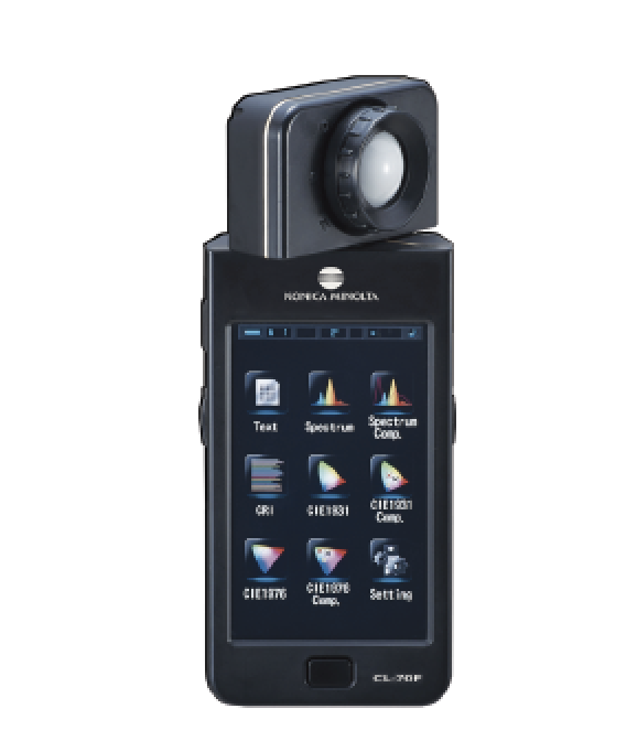
Figure 1. CL-70F CRI Illuminance Meter
Additionally, Konica Minolta Sensing Americas, Inc. will have on display at LEDucation 2019 its widely received
CS-150 and CS-160 Luminance and Color Meters, as well as CL-200A Chroma Meter and its imaging measurement system,
LumiCam 2400 sold by Konica Minolta’s Instrument Systems.
To read more information on Konica Minolta Sensing Americas, Inc. products, visit us at:
/us/products/cs-150-luminance-and-color-meter/
Company profile of Konica Minolta Sensing Americas
Konica Minolta Sensing Americas, Inc. (KMSA), a wholly owned subsidiary of Konica Minolta, Inc., Sensing Business Unit is recognized as the international leader of industrial color and light measurement. The company is responsible for product lines that continuously revolutionize how visual perception is measured by the world.
Konica Minolta Sensing Americas' Ramsey, New Jersey corporate headquarters is fully equipped with a state of the art service center, technical support center, and a focused sales force dedicated to both the North American and South American regions. When it comes to color and light measurement, the world looks to Konica Minolta.
Contact:
Peter Roos, Marketing Manager
Konica Minolta Sensing Americas
Phone: (201) 236-4300
Toll Free: (888) 473-2625
Web: https://sensing.konicaminolta.us/us
Email: marketing.sus@konicaminolta.com
Terms and product names may be trademarks or registered trademarks of their respective holders and are hereby acknowledged.
Konica Minolta Sensing Americas, Inc. to Showcase Advanced Light Measurement Solutions at LEDucation 2019.
January 2019 – Konica Minolta Sensing Americas, Inc. is pleased to announce that we will be exhibiting our luminance and
color meters CS-150 and CS-160 at LEDucation 2019, March 12-13 2019.
CS-150 and CS-160 are the successors to the CS-100 (launched in 1986) and CS-100A (launched in 2000) and are capable of
measuring chromaticity, luminance, and correlated color temperature values to help ensure the stable quality of various light
sources in terms of brightness and color.
The CS-150 is a highly accurate tristimulus colorimeter equipped with newly designed sensors with spectral responses that
more closely match the CIE 1931 color-matching functions representing the sensitivity of the human eye to provide
measurement results that better correlate with visual evaluation. The CS-150 luminance and color meter allows luminance and
chromaticity to be measured remotely with an acceptance angle of 1°.
The CS-160 is a lightweight, compact and battery powered luminance and tristimulus colorimeter for the measurement of a
wide range of luminance conditions and non-contact measurement of color. The CS-160 luminance and color meter allows
luminance and chromaticity to be measured remotely with an acceptance angle of 1/3° for small light-emitting surfaces. The
CS-160 provides an increased measurement range and a sensor that more closely matches the CIE 1931 color-matching
functions.
Konica Minolta Sensing Americas, Inc.’s measurement instruments are built with cutting edge technology and held to the
strictest accuracy and quality. Both instruments are the perfect marriage of efficiency and ergonomics with regards to spot
measurements in a handheld portable instrument.
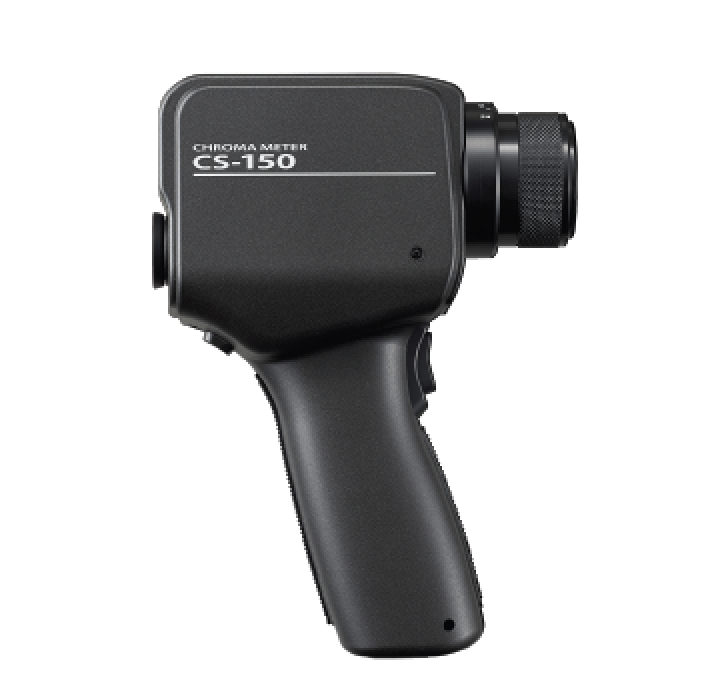
Figure 1. CS-150 Luminance and Color Meter
Additionally, Konica Minolta Sensing Americas, Inc. will have on display at LEDucation 2019 its cost-effective spectrometerbased
illuminance meter CL-70F, as well as CL-200A Chroma Meter and its imaging measurement system, LumiCam 2400 sold
by Konica Minolta’s Instrument Systems.
To read more information on Konica Minolta Sensing Americas, Inc. products, visit us at:
/us/products/cs-150-luminance-and-color-meter/
Company profile of Konica Minolta Sensing Americas
Konica Minolta Sensing Americas, Inc. (KMSA), a wholly owned subsidiary of Konica Minolta, Inc., Sensing Business Unit is recognized as the international leader of industrial color and light measurement. The company is responsible for product lines that continuously revolutionize how visual perception is measured by the world.
Konica Minolta Sensing Americas' Ramsey, New Jersey corporate headquarters is fully equipped with a state of the art service center, technical support center, and a focused sales force dedicated to both the North American and South American regions. When it comes to color and light measurement, the world looks to Konica Minolta.
Contact:
Peter Roos, Marketing Manager
Konica Minolta Sensing Americas
Phone: (201) 236-4300
Toll Free: (888) 473-2625
Web: https://sensing.konicaminolta.us/us
Email: marketing.sus@konicaminolta.com
Terms and product names may be trademarks or registered trademarks of their respective holders and are hereby acknowledged.