Pushing the Limits of TV Displays with MicroLED Provides No Boundaries

MicroLEDs are really tiny LEDs… micro in size, typically 1/10th the width of a human hair, measuring less than 100um. They are much smaller than what is presently found in today’s LCD TVs, flashlights or lightbulbs. The individual LEDs are self-emissive (self-radiant), each featuring millions of individual colors. Each LED chip individually produces its own brilliant colored light, similar to that of the LED technology found in OLEDs. But, unlike the present OLEDs it does not rely on organic elements to produce its own light but rather uses an inorganic material known as Gallium Nitride. The use of this inorganic material allows for devices or panels to be made thinner because it does not require a polarizing or an encapsulation layer. Like its ‘older sibling’, MicroLED also offers high contrast ratios allowing for deeper blacks but without the potential for image retention or ‘burn-in. It also offers ‘deep blacks’, superior color, and exceptional angular viewing. The benefits of MicroLED is where they differ. MicroLEDs are brighter, have a faster response time, longer lifespan expectancy, and has modular capabilities allowing for additional panels at irregular sizes to be added without compromising picture quality.
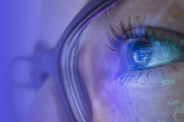
As major manufacturers address the possibilities of the new MicroLED technology, luminance efficiency issues come to question. As a leader in the light and display industry, many turn to Konica Minolta Sensing to provide them with the instrument and tools needed to accurately measure photometric brightness and color.
In comparing MicroLED to OLED the difference is shown in MicroLED’s makeup. The infrastructure of the materials used with MicroLEDs, leans itself to the ability for the panels to be extremely thin in its width, measuring less than 100µm (less than the width of a strand of hair!). In addition, an impressive feature of bezel-free MicroLED displays is that it allows for no borders between modules even if one decides to add more at a later date. The impression of a borderless display is seamless, literally! This concept allows for numerous panels to be used in an assortment of sizes. Now one can create a digital image from the standard 16:9 content to 21:9 widescreen films, to the more unconventional ratios of 32:9, or even 1:1 without altering the quality of the displayed image. This unique flexibility in screen size coupled with the feature of being bezel-free allows for the adaptation to fit any room or size without the nuisance of borders or seams between each panel and at the same time keeping the same quality resolution.
Challenges?
Surprisingly, the biggest challenge of MicroLEDs is not image quality but rather in its manufacturing. MicroLED displays are much more difficult to produce. This difficulty is mostly due to the shrinking of the LEDs. Typically, as you shrink the size of a LED you also diminish the level of brightness it produces. In order to shrink the LED and still have the same amount of brightness, an increase in energy is then needed for it to have it perform at its fullest capacity. Therefore, historically the issue of efficiency becomes a dilemma. Increasing the LED’s output increases the electricity used and heat emitted. This in turn, increases energy costs as well as every manufacturer’s nightmare-the potential issue of overheating. This is where MicroLED technology differs and excels. The MicroLED technology addresses this issue and has successfully made efficient LEDs at a fraction of the size without the transmission of heat. The 2nd challenge is the limitations on how much one can shrink the gap between the pixels and the relative circuits and electronic elements that are to be used for the display being created. This can create a challenge when 25 million LEDs are required and then are grouped into modules in order to produce the desired output. This is best understood when you compare this to a few dozen yellow-blue ‘white’ LEDS that today’s typical 4K display sized at 3,840 x 2,160 requires. This attention to detail increases the cost of production. The increase is approximately 4 times more than what it costs to produce an OLED panel. This cost may inhibit the adoption of this technology by manufacturers as they might be reluctant to make the investment in the expensive machinery and complicated production processes used to produce these MicroLED panels.
Some leaders in the industry feel the ultimate goal is to make a 4K resolution into a smaller format that can be used in a variety of industries and make it financially adaptable. The challenge is how to make a display smaller and more efficient without sacrificing brightness at a price the average consumer might be able to afford?
Why is this technology so much better?
In a nutshell, MicroLEDs are currently brighter than any other display technology that currently exists. It has a wide spectrum of color, provides deeper contrasts in blacks, nearly eliminates the issue of distortions from viewing at different angles, has an extremely fast response times and is energy efficient as it can operate at very bright settings without producing much heat. How much more energy efficient is it? Consumption is 90% lower than LCD and 50% lower than OLED. This substantial savings in energy can be a potential benefit for cellphone manufacturers as they find their battery life capabilities increase dramatically. Additionally, the benefit of increased speed can be seen best in VR technology. Presently, the speed for VR applications using OLEDs are in the range of microseconds. In contrast, the MicroLED technology can run the same program to that of nanospeed, which is 1000 times faster! Don’t blink!
What might the future hold?
One might expect to see this technology first available commercially rather than at a consumer level. Although the possibilities of end-uses are limitless, the cost currently is not feasible for the average consumer. MicroLEDs are still in its infancy stage as more patents and investments can be seen being made by several big players in a variety of industries. This can be seen as powerful players unveiled their advancements highlighting this new MicroLED technology in the display market at the CES tradeshow in Las Vegas this past January. In addition, discussions in the medical field for use of MicroLEDs in optogenetics applications is just at the beginning of its marketability. The potential for adaptability into other industries is likely as there is still much to learn about all the application potentials of this technology and the likelihood of other corporations jumping onboard in its future are anticipated.
The cost of production of the MicroLEDs are expected to be 4 times higher than current LCD and OLED panels. This increase is directly correlated to the demand of higher resolutions and the cost of accuracy needed in the soldering process to achieve this. Although there is a definite interest in the MicroLED technology, many manufactures are preoccupied in the latest OLED technology and are not ready to shift gears into adopting a new format. The reality of MicroLEDs becoming financially feasible available to the general market, (other than the home luxury market) is not likely in the immediate future. But consumers shouldn’t be weary, the recently made available OLED technology is now being mass produced for individual use at a much more affordable price and is nothing short of remarkably impressive, offering a huge leap from that of LCD technology.
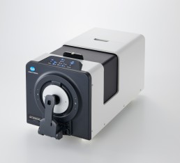
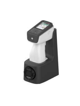
To maintain a consistency of quality in the production of their displays MicroLED manufacturers often require the innovative display measurement technology available from Konica Minolta Sensing. Industry-leading instruments such as the CS-150 luminance and color meter, CS-3000 Spectroradiometer, and our newest addition our CA-410 display color analyzer probe with a range of luminance up to 30k cd/m2 and frequency up to 240Hz used for display calibrations offering highly precise measurements of the color and light qualities of display screens and assist manufacturers in creating a more visually satisfying product. Discover the difference that the display measurement technology from Konica Minolta Sensing can make today!
Sources:
https://www.cnet.com/news/microled-oled-screen-technology-samsung-the-wall/
- D. Dawson and M. A. A. Neil, “Micro-pixelated LEDs for Science and Instrumentation” J Phys D. 41 090301 (2008); V. Poher, N. Grossman, G. T. Kennedy, K. Nikolic, H. X. Zhang, Z. Gong, E. M. Drakakis, E. Gu, M. D. Dawson, P. M. W. French, P. Degenaar, and M. A. Neil, “Micro-LED arrays: a tool for two-dimensional neuron stimulation,” J. Phys. D Appl. Phys. 41(9), 094014 (2008).
https://www.androidauthority.com/micro-led-display-explained-805148/
https://news.samsung.com/us/samsung-unveils-modular-micro-led-technology-ces-2019/
https://www.digitaltrends.com/home-theater/microled-vs-oled/
https://www.flatpanelshd.com/focus.php?subaction=showfull&id=1477048275
https://wccftech.com/microled-vs-oled-everything-explained/